SKYLAB Long Distance ARM-M4 Core bluetooth dongle 5.0,bluetooth 5.0 dongle,nRF52 nrf52840 bluetooth 5.0 module
QUESTIONS & ANSWERS
Have a Question?
Be the first to ask a question about this.
Share this Product

![]()
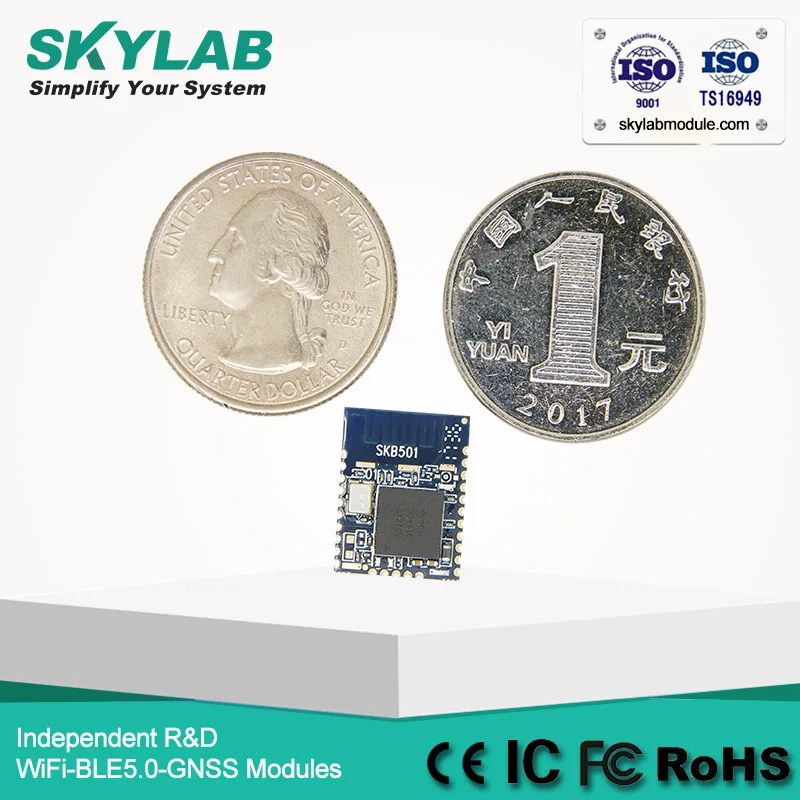
Name: SKYLAB Long Distance ARM-M4 Core bluetooth dongle 5.0,bluetooth 5.0 dongle,nRF52 nrf52840 bluetooth 5.0 module
Model No.: SKB501

Ready for Bluetooth 5 and high grade IoT security
The SKB501 is an advanced, highly flexible single chip solution for today’s increasingly demanding ULP wireless applications for connected devices on our person, connected living environments and the IoT at large. It is designed ready for the major feature advancements of Bluetooth® 5 and takes advantage of Bluetooth 5’s increased performance capabilities which include long range and high throughput modes. Inherent industry-grade security is essential in today’s applications.
Bluetooth 5 – Bluetooth low energy further and faster
The nRF52840 is ready to take advantage of the considerable performance improvements for Bluetooth low energy with the arrival of the Bluetooth 5 specification. Of greatest importance is the support for longer range (up to x4 compared to Bluetooth 4.x) and doubling of on-air data-rate, up to 2Mbs from 1Mbs in Bluetooth 4.x
Wide protocol support with addition of 802.15.4
The 802.15.4 PHY and MAC layers are supported natively on the nRF52840. This allows nRF52840 to be used in a wide range of home and industrial sensor network applications as it supports two of the most popular wireless sensor standards in use today, Bluetooth low energy and 802.15.4 derivatives. This adds to the already existing radio support for Bluetooth low energy, ANT/ANT+ and 2.4GHz for proprietary.
![]()
Features
◆Bluetooth 5 ready multi-protocol radio
◆Bluetooth 5 datarate support: 2Mbs, 1Mbs, 500Kbs, 125Kbs
◆Support ANT Protocol
◆32-bit ARM Cortex-M4F @ 64MHz
◆Up to 111 dB link budget for Bluetooth long range mode
◆NFC-A on-chip
◆Programmable output power from +8dBm to -20dBm
◆-96dBm Sensitivity for Bluetooth low energy
◆RSSI
◆Wide supply voltage range +5.5v to 1.7v
◆Full selection of interfaces SPI/UART/PWM
◆Programmable Peripheral Interface - PPI
◆High speed SPI interface 32MHz
◆EasyDMA for all digital interfaces
◆12bit/200K SPS ADC
◆128 bit AES/ECB/CCM/AAR co-processor
◆20 General Purpose I/O pins
◆SPI Master/Slave
◆Two-wire Master (I2C compatible)
◆UART (CTS/RTS)
◆RoHS compliance (Lead-free)
◆FCC,CE compliance
![]()
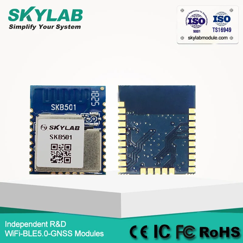
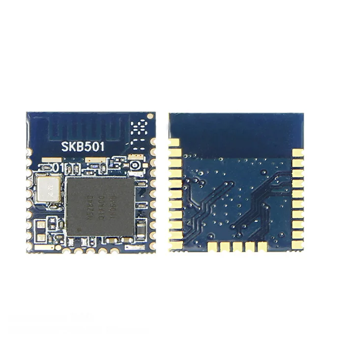
Dimesion: 17.4(L) x 13.7(W) x 1.9(H) mm

5. Interfaces
5.1 Power Supply
Regulated power for the SKB501 is required. The input voltage Vcc range should be 1.7V to 3.6V. Suitable decoupling must be provided by external decoupling circuitry (10uF and 0.1uF). It can reduce the noise from power supply and increase power stability.
5.2 System Function Interfaces
5.2.1 GPIOs
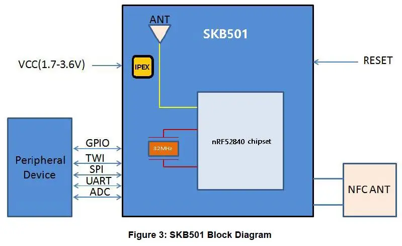
The general purpose I/O is organized as one port with up to 20 I/Os enabling access and control of up to 19 pins through one port. Each GPIO can be accessed individually with the following user configurable features:
1、Input/output direction
2、Output drive strength
3、Internal pull-up and pull-down resistors
4、Wake-up from high or low level triggers on all pins
5、Trigger interrupt on all pins
6、All pins can be used by the PPI task/event system; the maximum number of pins that
can be interfaced through the PPI at the same time is limited by the number of GPIOTE channels
7、All pins can be individually configured to carry serial interface or quadrature demodulator signals
8、All pins can be configured as PWM signal.
9、There are 6 ADC/LPCOMP input in the 20 I/Os.
5.2.2 Two-wire Interface (I2C Compatible)
The two-wire interface can communicate with a bi-directional wired-AND bus with two lines (SCL, SDA). The protocol makes it possible to interconnect up to 127 individually addressable devices. The interface is capable of clock stretching, supporting data rates of 100 kbps ,250kbps and 400 kbps. The module has 2 TWI ports and they properties like following table.
5.2.3 Flash Program I/Os
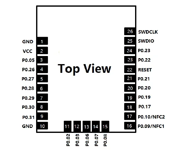
The module has two programmer pins, respectively SWDCLK pin and SWDIO pin. The two pin Serial Wire Debug (SWD) interface provided as a part of the Debug Access Port (DAP) offers a flexible and powerful mechanism for non-intrusive debugging of program code. Breakpoints and single stepping are part of this support.
5.2.4 Serial Peripheral Interface
The SPI interfaces enable full duplex synchronous communication between devices. They support a three-wire (SCK, MISO, MOSI) bi-directional bus with fast data transfers. The SPI Master can communicate with multiple slaves using individual chip select signals for each of the slave devices attached to a bus. Control of chip select signals is left to the application through use of GPIO signals. SPI Master has double buffered I/O data. The SPI Slave includes EasyDMA for data transfer directly to and from RAM allowing Slave data transfers to occur while the CPU is IDLE. The GPIOs are used for each SPI interface line can be chosen from any GPIOs on the device and configed independently. This enables great flexibility in device pinout and efficient use of printed circuit board space and signal routing.
5.2.5 UARTs
The Universal Asynchronous Receiver/Transmitter offers fast, full-duplex, asynchronous serial communication with built-in flow control (CTS, RTS), support in hardware up to 1 Mbps baud. Parity checking is supported.
Support the following baudrate in bps unit: 1200/2400/4800/9600/14400/19200/28800/38400/57600/76800/115200.
Note: The GPIOs are used for each SPI/TWI/UART interface line can be chosen from any GPIOs on the device and configed independently.
5.2.6 Analog to Digital Converter (ADC)
The 12 bit incremental Analog to Digital Converter (ADC) enables sampling of up to 8 external signals through a front-end multiplexer. The ADC has configurable input and reference prescaling, and sample resolution (8,10, and 12 bit).
5.2.7 Low Power Comparator (LPCOMP)
In System ON, the block can generate separate events on rising and falling edges of a signal, or sample the current state of the pin as being above or below the threshold. The block can be configured to use any of the analog inputs on the device. Additionally, the low power comparator can be used as an analog wakeup source from System OFF or System ON. The comparator threshold can be programmed to a range of fractions of the supply voltage.
5.2.8 Reset
The reset pin of the SKB501 module is in the internal pull-high state , when the reset pin of the
module is input to a low level , the module will be automatically reset .After the reset pin is used , the parameters of the current setting will not be ANT .
5.2.9 NFC
The NFC peripheral (referred to as the 'NFC peripheral' from now on) supports communication signal interface type A and 106 kbps bit rate from the NFC Forum.
With appropriate software, the NFC peripheral can be used to emulate the listening device NFC-A as specified by the NFC Forum.
Listed here are the main features for the NFC peripheral:
• NFC-A listen mode operation
• 13.56 MHz input frequency
• Bit rate 106 kbps
• Wake-on-field low power field detection (SENSE) mode
• Frame assemble and disassemble for the NFC-A frames specified by the NFC Forum
• Programmable frame timing controller
• Integrated automatic collision resolution, CRC and parity functions


![[variant_title] - SKYLAB Long Distance ARM-M4 Core bluetooth dongle 5.0,bluetooth 5.0 dongle,nRF52 nrf52840 bluetooth 5.0 module](http://smartdevice.pk/cdn/shop/products/HTB1slBFLxnaK1RjSZFBq6AW7VXaQ_180x.jpg?v=1569827985)
![[variant_title] - SKYLAB Long Distance ARM-M4 Core bluetooth dongle 5.0,bluetooth 5.0 dongle,nRF52 nrf52840 bluetooth 5.0 module](http://smartdevice.pk/cdn/shop/products/HTB1AEhhLpYqK1RjSZLeq6zXppXaa_{width}x.jpg?v=1569827985)
![[variant_title] - SKYLAB Long Distance ARM-M4 Core bluetooth dongle 5.0,bluetooth 5.0 dongle,nRF52 nrf52840 bluetooth 5.0 module](http://smartdevice.pk/cdn/shop/products/HTB1rXXhLrvpK1RjSZFqq6AXUVXa4_{width}x.jpg?v=1569827985)
![[variant_title] - SKYLAB Long Distance ARM-M4 Core bluetooth dongle 5.0,bluetooth 5.0 dongle,nRF52 nrf52840 bluetooth 5.0 module](http://smartdevice.pk/cdn/shop/products/HTB1X84uLxjaK1RjSZFAq6zdLFXad_{width}x.jpg?v=1569827985)

![[variant_title] - SKYLAB Long Distance ARM-M4 Core bluetooth dongle 5.0,bluetooth 5.0 dongle,nRF52 nrf52840 bluetooth 5.0 module](http://smartdevice.pk/cdn/shop/products/HTB1slBFLxnaK1RjSZFBq6AW7VXaQ_grande.jpg?v=1569827985)
![[variant_title] - SKYLAB Long Distance ARM-M4 Core bluetooth dongle 5.0,bluetooth 5.0 dongle,nRF52 nrf52840 bluetooth 5.0 module](http://smartdevice.pk/cdn/shop/products/HTB1AEhhLpYqK1RjSZLeq6zXppXaa_grande.jpg?v=1569827985)
![[variant_title] - SKYLAB Long Distance ARM-M4 Core bluetooth dongle 5.0,bluetooth 5.0 dongle,nRF52 nrf52840 bluetooth 5.0 module](http://smartdevice.pk/cdn/shop/products/HTB1rXXhLrvpK1RjSZFqq6AXUVXa4_grande.jpg?v=1569827985)
![[variant_title] - SKYLAB Long Distance ARM-M4 Core bluetooth dongle 5.0,bluetooth 5.0 dongle,nRF52 nrf52840 bluetooth 5.0 module](http://smartdevice.pk/cdn/shop/products/HTB1X84uLxjaK1RjSZFAq6zdLFXad_grande.jpg?v=1569827985)


![[variant_title] - (1piece/lot) PMI8952 000 PM8937 0VV PM8941 0VV PM8952 001 PMI8937 PM8953 PM8940 PMI8994 002 PM8953 PMI8940](http://smartdevice.pk/cdn/shop/products/HTB1ob66ncj_B1NjSZFHq6yDWpXa6_{width}x.jpg?v=1569821702)